Restoring the magic in design
About fifty years later, Integrated Circuits are everywhere. Yet, the process of creating these amazing devices feels somewhat tired. CMOS scaling, the engine behind the evolution in complexity over all these decades, is slowing down and will most likely peter out in about a decade. So has innovation in design tools and methodologies. As a consequence, the lure of IC design and design tool development has faded, causing a talent shortage worldwide. Yet, at the same time, this moment of transition offers a world of opportunity and excitement. Novel technologies and devices, integrated in three-dimensional artifacts are emerging and are opening the door for truly transformational applications such as brain-machine interfaces and swarms of nanobots. Machine learning, artificial intelligence, optical and quantum computing present novel models of computation surpassing the instruction-set processor paradigm. With this comes a need again to re-invent the design process, explicitly exploiting the capabilities offered by this next generation of computing systems. In summary, it is time to put the magic in design again.
Jan is a Professor in the Graduate School in the EECS Department the University of California at Berkeley, after being the holder of the Donald O. Pederson Distinguished Professorship at the same institute for over 30 years. He is a founding director of the Berkeley Wireless Research Center (BWRC) and the Berkeley Ubiquitous SwarmLab, and has served as the Electrical Engineering Division Chair at Berkeley twice. In 2019, he also became the CTO of the System-Technology Co-Optimization (STCO) Division of IMEC, Belgium.
Prof. Rabaey has made high-impact contributions to a number of fields, including low power integrated circuits, advanced wireless systems, mobile devices, sensor networks, and ubiquitous computing. Some of the systems he helped envision include the infoPad (a forerunner of the iPad), PicoNets and PicoRadios (IoT avant-la-lettre), the Swarm (IoT on steroids), Brain-Machine interfaces and the Human Intranet. His current interests include the conception of the next-generation distributed systems, as well as the exploration of the interaction between the cyber and the biological worlds.
He is the primary author of the influential “Digital Integrated Circuits: A Design Perspective” textbook that has served to educate hundreds of thousands of students all over the world. He is the recipient of numerous awards, is a Life Fellow of the IEEE, and has been involved in a broad variety of start-up ventures.
Innovative systems for railway infrastructure managment
From Nano-Drones to Cars - A RISC-V Open Platform for next-generation Vehicles
Luca Benini holds the chair of digital Circuits and systems at ETHZ and is Full Professor at the Universita di Bologna. He received a PhD from Stanford University. Dr. Benini's research interests are in energy-efficient parallel computing systems, smart sensing micro-systems and machine learning hardware. He is a Fellow of the IEEE, of the ACM and a member of the Academia Europaea. He is the recipient of the 2016 IEEE CAS Mac Van Valkenburg award, the 2020 EDAA achievement Award and the 2020 ACM/IEEE A. Richard Newton Award.
Thin film electronic devices marry lab-on-chip applications
After a review on the actual trends in lab-on-chip technology, this talk focuses on true la-on-chip, where thin film sensors and actuators are combined in a multifunctional optoelectronic platform. In particular, the platform integrates amorphous silicon sensors for on-chip detection and temperature control and optical filters for selection of specified wavelength. By coupling this platform with a microfluidic network, this platform enables application in the field of mycotoxin detection and DNA amplification of bacteria and virus.
Domenico Caputo is Associate Professor with tenure at Sapienza University of Rome. He teaches "Electronics" for Clinical Engineering and "Biomedical Equipment and Techniques" for Biomedical Engineering.
Domenico Caputo is the Scientific Responsible of the laboratories for optoelectronic characterization of thin film material and devices. His main research fields have been focused on the development of amorphous silicon electronic devices and photosensors and their integration on optoelectronic system-on-glass.
He is coauthor of more than 120 papers on international high-ranking journals and more than 140 proceedings of international conferences. He is referee of several scientific journals in the field of both electronic and biomedical devices and has been chairman of several international conferences. He has been Scientific Responsible of numerous National and International projects including two European projects and a Bilateral Project with the People’s Republic of China. The present research activity concerns the development of lab-on-chip system for biomedical applications based on thin film devices. In particular, he has developed and integrated thin film temperature sensors and photosensors in miniaturized lab-on-chip for DNA analysis and mycotoxin detection.
State-of-the-art and trends of silicon detector technology for particle physics
Gianluigi Casse is scientist especially active in the field of instrumentation for particle physics. He worked at CERN and at the University of Liverpool where he holds a chair in experimental particle physics. He has been involved in detector development for a number of important systems for several high energy physics experiments. He has contributed to CDF at Fermilab, and to the ATLAS and LHCb experiments at the CERN LHC. He is currently part of the LHCb Experiment at CERN, for which he gave a substantial contribution to the design, production and commissioning of the Vertex Locator (VELO). He has contributed to the design of the ATLAS silicon tracker detector and its upgrades (currently in progress). He is Spokes-person of the CERN/RD50 experiment at CERN that counts over 400 scientists from 66 institutes worldwide, aimed at the development of novel and extremely radiation tolerant instrumentation for future high-energy physics experiments. He has been leading the R&D for the Liverpool group from 2010. From 2016 to 2021 he served two terms as the director of the Centre for Sensors and Devices of the Fondazione Bruno Kessler (FBK) in Trento, which is a major player in Italy for the development of advanced sensor for scientific experiments and instrumentation.
Addressable Monolithic InSb on GaAs Focal Plane Arrays for MWIR Imaging
David Cumming is the Professor of Electronic Systems at the University of Glasgow. He completed a B.Eng in Electronics and Electrical Engineering at the University of Glasgow in 1989 and a Ph.D. in microelectronics at the University of Cambridge in 1993. He subsequently worked as a VLSI design engineer with STMicroelectronics in Bristol, UK, and carried out post-doctoral research at Glasgow University. He was a lecturer at the University of Canterbury, NZ, from 1997-1999, when he returned to Glasgow University. His research interests are focused on semiconductor devices and microsystems for sensing applications. He has published over 300 papers on sensor and photonic technologies, mainly with an emphasis on integration of technologies for a range of applications. His research on CMOS ion sensor arrays enabled the development of the Ion Torrent gene sequencing system. He has held 1851 and EPSRC research fellowships, a Chinese Academy of Science Distinguished Research Fellowship and held a Royal Society Wolfson Merit Award. He has been elected Fellow of the Royal Society of Edinburgh, Fellow of the Royal Academy of Engineering and Fellow of the Institute of Electrical and Electronics Engineers.
Neuromorphic computing in the edge: merging cyber and physical
Georges G.E. Gielen received the MSc and PhD degrees in Electrical Engineering from the Katholieke Universiteit Leuven (KU Leuven), Belgium, in 1986 and 1990, respectively. He is Full Professor in the MICAS research division at the Department of Electrical Engineering (ESAT). From August 2013 till July 2017 he was also appointed at KU Leuven as Vice‐Rector for the Group of Sciences, Engineering and Technology, and he was also responsible for academic Human Resource Management. His research interests are in the design of analog and mixed‐signal integrated circuits, and especially in analog and mixed‐signal CAD tools and design automation. He is a frequently invited speaker/lecturer and coordinator/partner of several (industrial) research projects in this area, including several European projects. He has (co‐)authored 10 books and more than 600 papers in edited books, international journals and conference proceedings. He is Fellow of the IEEE since 2002, and received the IEEE CAS Mac Van Valkenburg career award in 2015. He is a 1997 Laureate of the Belgian Royal Academy of Sciences, Literature and Arts in the discipline of Engineering.
Quo Vadis IC System Design?
Alberto Sangiovanni Vincentelli is the Edgar L. and Harold H. Buttner Chair of Electrical Engineering and Computer Sciences at the University of California at Berkeley. He is an author of over 1000 papers, 17 books and 2 patents in the area of design tools and methodologies, large scale systems, embedded systems, hybrid systems and innovation.
He was a co-founder of Cadence and Synopsys, the two leading companies in the area of Electronic Design Automation. He is a member of the Board of Directors of both public and privately held companies. He was a consultant or member of the Adviosry Boards of of several tech companies such as BMW, Mercedes, Magneti Marelli, Intel, ST microelectronics, HP, General Motors, United Technologies, Lutron, Lendlease and Elettronica. Currently, he is a member of the following boards/committees: Advisory Board, Xseed; Investment Committee of Indaco Ventures and Fondo Next. Board of Directors: Cadence, KPIT Technologies, eGap, Exein, Cy4Gate. He is Chairman of the Board of Quantum Motion, Innatera, Phoelex, e4Life and Phononic Vibes. From January 2013 to 2016, he was the President of the Strategic Committee of the Italian Strategic Fund. He was member of the Scientific Council of the Italian National Science Foundation (CNR) from 2001 to 2015. From February 2010 to December 2020, he had been a member of the Executive Committee of the Italian Institute of Technology, where he is now a member of the Technical Scientific Committee. From July 2012 to July 2015, he was Chairperson of the Comitato Nazionale Garanti per la Ricerca. He is the Chairperson of the Strategy Board and of the International advisory Board of the Milano Innovation District (MIND)
He is the recipient of several academic honors, research awards and honorary degrees including the IEEE/RSE Wolfson James Clerk Maxwell Medal “for groundbreaking contributions that have had an exceptional impact on the development of electronics and electrical engineering or related fields”. Alberto obtained an electrical engineering and computer science degree (“Dottore in Ingegneria”) summa cum laude from the Politecnico di Milano, Italy in 1971 and holds four Honorary Doctorates from University of Aalborg, KTH, AGH and University of Rome, Tor Vergata.
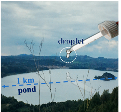
Single-protein large area detections: from mechanism to applications in the clinics
...like spotting a droplet of water falling on the surface of a 1 Km wide lake.
The applications span from a handheld intelligent single-molecule binary bioelectronic system for fast and reliable immunometric point-of-care testing of COVID-18 patients [3] and Xylella fastidiosa single bacterium detected in infected plants sap. The phenomenon enabling such outstanding performance level was discovered in 2018 [4]. While still under investigation, it is supposed to involve an amplification that starts from the single affinity binding that triggers a propagating collaborative response.
Future actions include the deepening of our understanding of the sensing mechanism and the engagement in a campaign of thousands of clinical trials that will bring SiMoT beyond TRL5.
- E. Macchia et al. Chemical Review 2022, 122, 4636 DOI: 10.1021/acs.chemrev.1c00290
- E. Macchia et al. Advanced Science 2022, 2104381 DOI: DOI: 10.1002/advs.2021043811
- E. Macchia et al., Science Advances 2022, 8 (27) DOI: 10.1126/sciadv.abo0881
- E. Macchia et al., Nature Communication 2018, DOI: 10.1038/s41467-018-05235-z
Luisa Torsi received her Laurea degree in Physics from the University of Bari in 1989 and a Ph.D. in Chemical Sciences from the same institution in 1993. She was a post-doctoral fellow at Bell Labs from 1994 to 1996. In 2005 and 2006 she was invited-professor at the University of Anger and Paris 7. Since 2005 she is a full professor of chemistry at the University of Bari and since 2017, she is an adjunct professor at the Abo Academy University in Finland.
In 2010 she has been awarded the Heinrich Emanuel Merck prize for analytical sciences, marking the first time the award has been given to a woman. The IUPAC - International Union of Pure and Applied Chemistry awarded her with the 2019 Distinguished Women in Chemistry or Chemical Engineering. The analytical chemistry division of the European Chemical Society (EuChemS) conferred her the Robert Kellner Lecturer 2019. Prof. Luisa Torsi is also the winner of the Wilhelm Exner Medal 2021, a prize awarded since 1921 by the Austrian Industrial Association to celebrate excellence in science. The Exner Medal awardees include also more than twenty Nobel prizes. The Italian President, Sergio Mattarella invited Prof. Torsi at the Quirinale to personally congratulate her on this award.
Since 2020 she has been appointed National Representative for the Marie Skłodowska-Curie Action of Horizon Europe by the Italian Minister for Education and Research. She is also past-president of the European Material Research Society, the first woman to serve in this role. Torsi has been also elected 2017 Fellow of this society, for pioneering work in the field of organic (bio) electronic sensors and their use for point-of-care testing. She is also Fellow of the Royal Society of Chemistry since 2022. Presently she is serving as Vice-President of the Scientific Committee of the Italian National Research Council.
Awarded research funding for over 30 million € comprises several European contracts as well as national and regional projects. She is coordinating the "Single molecule bio-electronic smart system array for clinical testing – SiMBiT" a H2020-ICT-2018-2020 research and innovation action working on liquid biopsy for pancreatic cancer early detection. She has also coordinated a “European Industrial Doctorate” Marie Curie project in collaboration with Merck and a Marie Curie ITN European network as well as several national PRIN projects; was also a principal investigator in an ICT STREP proposal. She has also been the scientific coordinator of a Structural Reinforcement PON Project awarded to UNIBA for 2012-2014 and is engaged with several other Structural Reinforcement PON projects.
Torsi has authored almost 230 ISI papers, including papers published in Science, Nature Materials, Nature Communications, PNAS, Advanced Materials, and is co-inventor of several international awarded patents. Her works gathered almost 15.500 Google scholar citations resulting in an h-index of 60. She has given over190 invited lectures, including almost 50 plenary and keynotes contributions to international conferences.
Prof. Torsi is committed to the role of model for younger women scientists. She has been giving several talks on this topic such as a TEDx talk. Prof. Torsi is one of the 100Experts a project led by Fondazione Bracco comprising an online databank with the names and CVs of female experts in STEM, a sector historically underrepresented by women but strategic for the economic and social development. In a recent campaign to foster the idea of gender equality in science among children, prof. Torsi was featured in a story of TOPOLINO (Italian comic digest-size series of Disney comics), as "Louise Torduck", a successful female scientist of the Calisota valley.
Ultra low power event-driven sensor interfaces
Pieter Harpe (SM'15) received the M.Sc. and Ph.D. degrees from the Eindhoven University of Technology, The Netherlands, in 2004 and 2010, respectively. In 2008, he started as researcher at Holst Centre / imec, The Netherlands. Since then, he has been working on ultra low-power wireless transceivers, with a main focus on ADC research and design. In April 2011, he joined Eindhoven University of Technology where he is currently an Associate Professor on low-power mixed-signal circuits. Dr. Harpe is analog subcommittee chair for the ESSCIRC conference and TPC member for A-SSCC. He also served as TPC member for ISSCC and AACD, was an IEEE SSCS Distinguished Lecturer and is recipient of the ISSCC 2015 Distinguished Technical Paper Award.
The Next Dawn for CMOS: Cryogenic ICs for Quantum Computing
For a functional quantum processor, an electronic interface to control operations on qubits and sense the results, is needed; today it is implemented with standard instrumentation placed at room temperature. This may work as proof of concept for the low number of qubits available today but not when the number of qubits will grow to hundreds of thousands or maybe millions as needed for the solution of practical problems, making room-temperature electronics for control unworkable due to the wiring requirements, signal integrity and cost.
The solution is to build the control electronics to operate at 4 K or below, close to the qubits. While many predict the gloom and doom of the end of Moore's scaling and implicitly semiconductor circuits, the application areas and the operating range of CMOS ICs keep expanding with no end in sight. Standard CMOS is the obvious technology of choice for quantum computing allowing both cryogenic operation (4 K down to 100 mK) and the integration on a single chip of the billions of transistors required to operate a very large number of qubits.
These circuits and systems must satisfy very stringent requirements for precise control of the qubit state and sensing tiny electrical signals with extreme accuracy while operating under a strict power budget below 1 mW/qubit imposed by the cooling limits of existing refrigeration technology.
The challenges and approach of designing and implementing integrated circuits (IC) operating at 4 K and below compatible with the qubits, will be described in this presentation along with the advantages of electron spin qubit implementations using the same semiconductor technology.
Andrei Vladimirescu (LF’17) received the M.S. and Ph.D. degrees in EECS from the University of California, Berkeley, where he was a key contributor to the SPICE simulator, releasing the SPICE2G6 production-level SW in 1981.
He pioneered electrical simulation on parallel computers with the CLASSIE simulator as part of his PhD. He is the author of "The SPICE Book" published by J. Wiley and Sons, that served to educate many generations of students worldwide.
For many years Andrei was R&D director leading the design and implementation of innovative Electronic Design Automation (EDA) products in software and hardware for Analog Devices Inc., Daisy Systems, Analog Design Tools, Valid Logic and Cadence. Currently he is Professor involved in research projects at the University of California at Berkeley and the Technical University of Delft as well as consultant to industry. His research activities are in the areas of low-voltage low-power CMOS, design, simulation and modeling, circuits with new devices and circuits for quantum computing.
Andrei is an IEEE Life Fellow and IEEE CASS Vice-president of Conferences.